To start the automatic layout generation, you must have finished your circuit schematic first. Please follow the Schematic Tutorial Example Lab #5 first if you have not done so.
This will overwrite the manual layout that has been drawn in Lab#7(Manual Layout). If you want to retain the manual layout, open the layout of the inverter and click on save as and give a different file name. You will be using the layout generated from this lab in the future lab exercises.
1. Open the schematic view of your design.
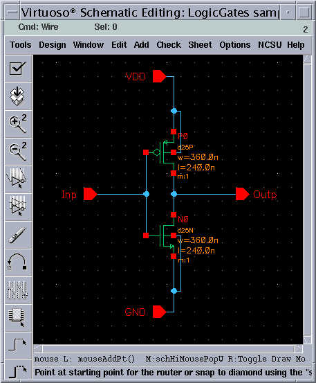
In this example, the PMOS transistor has a channel width of W=0.36u and a channel length of L=0.24u, while the NMOS transistor has a channel width of W=0.36u and a channel length of L=0.24u.
2. From the menu select Tools --> Design Synthesis --> Layout-XL.
Selecting this option will first open up a small dialog box that appears like the fig shown below.
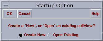
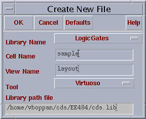
Up on selecting "Create New" a dialog box appears and will let the user select the cell name for the layout. It is a good idea to use the same cell name that the schematic has and specify layout as the cell view name.
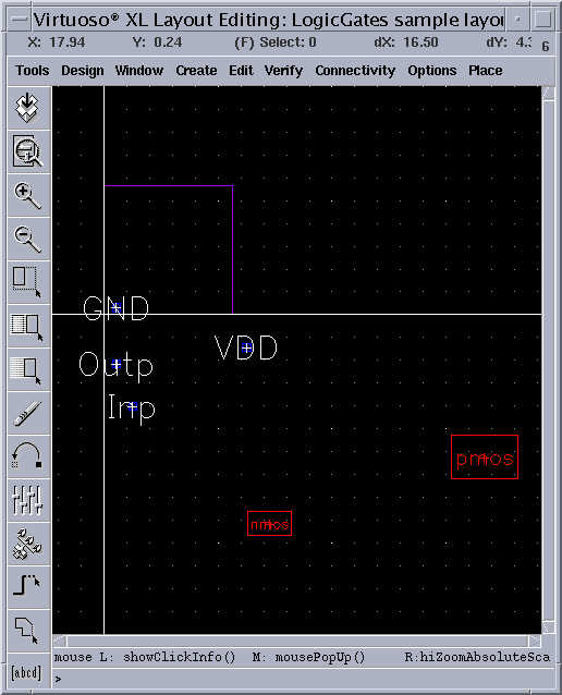
Upon the selection of the view name, In addition to the already open schematic window, a new layout window and the layer selection window will pop up. In the Layout window, select "Design -> Gen from Source" . This box will ask for a pin layer, pins in the layout will be placed as connections in the given layer. Choose Metal-1 as the I/O Pin Layer, and all of the pins that you have specified in your schematic will be placed as connections in Metal-1.
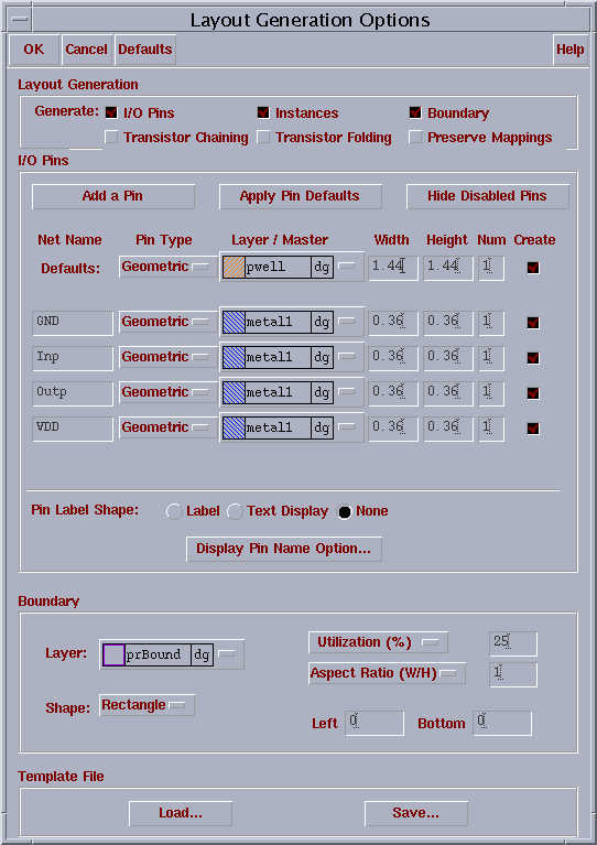
These three windows define the working environment for the automatic layout generation flow. If the names of the pins have to be listed on the layout window, Select "Label" and "Display Pin Name Option", the names of the pins will be displayed on the layout.( But do not do that because it gives "Design Rule Check Errors")
After the I/O pin layer is selected, two rectangles representing the transistors (the nmos and the pmos) and four Metal-1 squares will show up in the bottom half of the layout window. Notice the cyan colored square on the upper half of the layout window: This is the estimated size of the layout, this size is not mandatory, it is calculated roughly from the sizes of the active elements.( The window which you get will be different from what is shown below. Your window will not contain the label names of the pins. that's ok)
With the next step, you'll start forming the layout within the box above.