The default behavior of the layout editor is to show only the current hierarchy. You can press shift-f to display all the hierarchy levels, this way you'll be able to see actual transistors instead of the red instance rectangles.
The first step is to place all the components within the design area.
1. Select the PMOS transistor by clicking once
2. Move the selected transistor by dragging it with the mouse.
Note that in addition to the ghost image of the selected object, lines to other objects will show up. These lines represent the connections of the selected (and dragged) object to other objects of the design. In this example the poly of the PMOS transistor will be shown connected to the poly of the NMOS transistor and the input, and the drain region of the transistor will be shown connected to the output and the drain region of the NMOS.
3. Release the mouse button to place the selected transistor.
4. Move the remaining objects the same way
The figure after the PMOS and NMOS are moved in to the boundary is shown below.
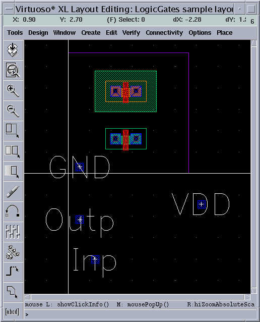
The Layout after the Input pin "Inp" and Output Pin "Outp" Metal-1 pins are moved in to the boundary is shown below.
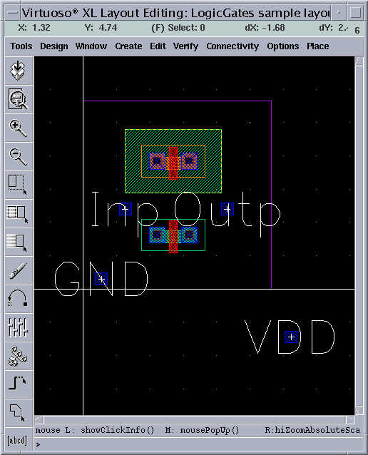
The Layout after the other two pins "VDD" and "Gnd" are placed in the boundary is shown below
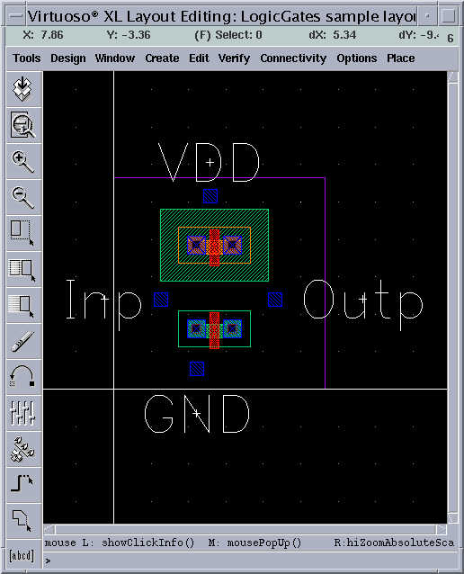
Your final Layout window should look more or less like this. Note that this placement is not obligatory, you can choose to place the transistors and the I/O pins any way you desire.