In the previous step we have placed the components, the next step is to make the connections between individual objects. We will be using the same methods that we used during manually drawing a layout here. The automatic layout tool has an additional menu which provides some useful options to facilitate signal connections.
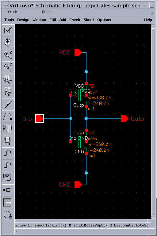
If we select the input pin in the layout, the input pin in the "schematic" window will be highlighted. You can go and select connections (nets) devices, and terminals in either layout or the schematic window and the corresponding object will be highlighted in the other window. This is called cross-probing.
As an example try clicking and selecting the Input pin connecting the gates of both transistors , notice that Input pin "Inp" in the layout window will be highlighted.
2. Connect the drain regions with Metal-1 using the path command.
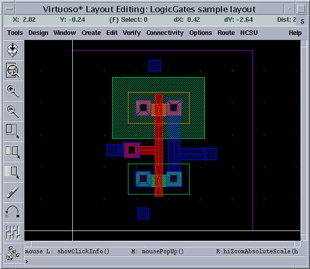
The figure after the Drains of the PMOS and NMOS are connected is shown below. After connecting the drains, place the output pin on the metal-1 wire drawn out.
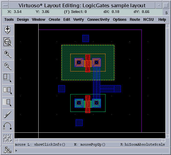
Connect the gates of both transistors using a poly path. The input must be in metal-1, so connect the poly and metal-1 by placing a via or interconnect that connects the metal-1 and poly layers. Instantiate "M1_POLY" as you have done in the manual layout example. Place the input pin on the metal-1 wire.