At this point the design is almost finished. Unfortunately the automatic design
creation process for this fabrication technology is unable to add substrate
connections. So these will have to be added by the user.
1. Using the Create --> Instance command select a "ptap" substrate contact.
For this case, the library will be "NCSU_TechLib_tsmc03d", the call name will be "ptap" and the view will be "Layout". Place the instance close to the bottom of the NMOS transistor, close to the source region
2. Using the Create --> Instance command select a "ntap" substrate contact.
This contact will be used as the n-well contact.
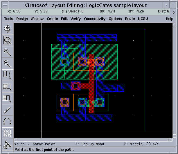
The figure after the "ptap" and the "ntap" are added is shown below
As in the previous manual layout example, the N-Substrate contact will not fit in a n-well that is drawn according to the minimum distance rules from the transistor. Since the transistor is an instance, it is not possible to stretch the n-well edge as it has been done in the layout example.
To address this problem, we can easily draw an extension to the already existing n-well using the rectangle command.

The next step is to draw the ground rail and the power rail.
3. Using the Path command draw the ground rail with Metal-1.
Make sure to connect the NMOS source and the substrate contact to the ground rail you have just drawn. Place the GND metal-1 pin on the ground rail.
4. Draw the power rail with Metal-1.
Place the VDD metal-1 pin on the power rail. This is the final layout, created by the automatic device level editor.