Note: The figures given may slightly change from what you see. They will be almost similar if not you will be helped
In this example, we did not pay much attention to the location of the transistors while building them. As long as the design rules are not violated, the transistors can be placed in any arbitrary arrangement. Yet based on our original signal flow diagram, it is more desirable to place the PMOS transistor directly on top of the NMOS transistor- for a more compact layout.
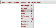
1. Select the PMOS transistor
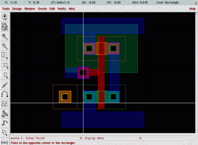
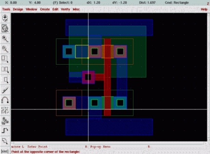
First make sure that you are in selection mode. If you are in any other mode (like rectangle drawing mode) exit the mode by pressing "ESC". Now using the mouse, click and drag a box that covers your PMOS. If you were successful, all the objects within the PMOS would be highlighted as in the figure below:
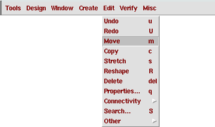
2. From the menu Edit select the option Move
( Edit --> Move )
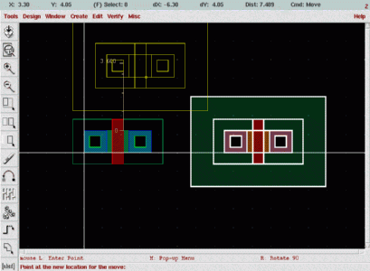
3. Pick the reference point
We will be asked to find a reference point for the object to be moved. The cursor will practically grab the object from that reference point. Since we want an accurate placement, it is advisable to select a point for which alignment is simpler. The corner between the diffusion and the poly is a good place to grab the PMOS.
After we have picked the reference point, the outline of the shape will appear attached to the cursor and we will be able to move the shape around. Since the minimum distance from diffusion to the n-well edge is 0.72u, the PMOS and NMOS have to be at least 1.44u apart (The distance between the active areas of PMOS and NMOS). We can place a ruler to help us aligning the two shapes and to measure the distance.
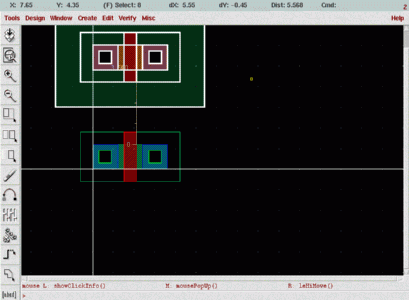
4. Place the transistor
You can drop the selected object (in this case consisting of the n-well, the p-active, poly and contacts) into its final location by clicking once on the left mouse button.
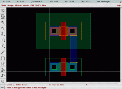
1. Draw a Metal-1 rectangle between NMOS and PMOS drain region contacts
Note that the minimum Metal-1 width is 0.36u (3 lambda), thus narrower than the Metal-1 covering the contacts. Also note that the transistors are completely symmetric, the source and drain regions are interchangeable.
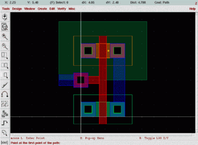
The next step will be to connect the gates of both transistors, which will form the input. To do this, we could use the rectangle command again, but this time we will use a different command, the path command. Throughout this tutorial, you will see that you typically have multiple options, commands or procedures available to create the same features in the layout. Please become familiar with as many of such options as possible.
1. Select poly layer from the LSW
![]()
2. From the Create menu select Path
( Create --> Path )
In the path mode you can draw lines (or paths) with the selected layer. The width of the drawn line can be adjusted, the default is the minimum width of the selected layer.
3. Start path
To start the path, click on the middle of the PMOS poly extension. You'll see a ghost line appear. Move this ghost line to the NMOS poly extension.
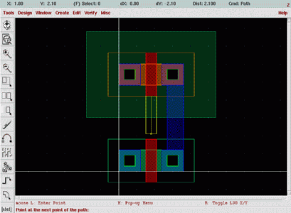
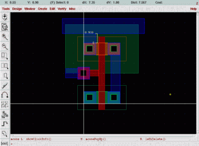
4. Double click to finish path
A single click will finish a line segment and let you continue drawing, a double click will finish the path.
We have already decided in our signal flow graph that we want the input in Metal-1. Therefore we have to make a connection from the poly layer to the Metal-1 layer.
This connection can be done manually by drawing a poly contact layer between Metal-1 and poly, but we will use the path command to automatically add the contacts.
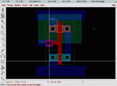
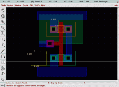
1. Starting from the poly line connecting the gates, start drawing a horizontal poly path.
We have to a connecter that will connect the metal-1 and poly layers.
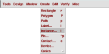
From the menu Create select option Instance
( Create --> Instance )
This will pop-up the instance options menu.
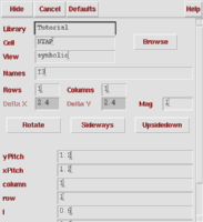
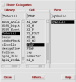
You'll have to provide a cell name and library here. It may be the case that you already know the cell name and cell view, but in this case it is better to Browse in your library to find the appropriate cell.
This is essentially the same library browser that you access when you start Cadence Design Tools. It lets you choose the library, cell and cell view, your selection will be transferred to the Instance options menu. For this case, the library will be "NCSU_TechLib_tsmc03d", the call name will be "M1_POLY" and the view will be "symbolic"
The Metal-1 & poly interconnect is named M1_POLY, and only has a layout view.
Select "Metal-1" in the LSW first. Select the "path" as explained in the above section and start path from the middle point of the contact.You can finish the path by double clicking.
By default, only the current layer of hierarchy is visible. Objects that you include as instances will be shown as boxes corresponding to their size. You can press SHIFT-F to see all levels of hierarchy. CTRL-F will return you to viewing only a single layer of hierarchy.
Now that our transistors are placed and connected, we will have to add Power and Ground rails. Usually a layout consists of a large number of cells, all of which need power and ground connections. Therefore it is common to design cells such that they will have one continuous, wide power and ground connection when placed side by side.
Our Signal Flow Graph suggests horizontal power and ground lines in Metal-1.
1. Draw the Power Rail in Metal-1 above the PMOS.
2. Draw the Ground Rail in Metal-1 below the NMOS
Make sure to connect the Power Rail and the Ground rail to the source contact of the PMOS and to that of NMOS, respectively.
The substrate on which the transistors are built must be properly biased. The way to do this is to add substrate contacts. The NMOS transistors are build on a p-type substrate, we will have to create a p-type substrate contact.
1. Draw a P-select square next to the NMOS transistor touching the nselect of the NMOS.
Since the contact will be made to p-substrate, the contact area will have to be p-type.(0.96um x 0.96um)
2. Draw a P-active square inside the P-select area.
This will define the active area of the substrate contact. make sure that you are not violating any design rules associated with active area spacing. Draw a square of 0.48um X 0.48um and it should be 0.24um (2 Lambda) from each side of the pselect.

3. Draw the active contact square inside the p-type active area. Select "CC layer". Draw a square 0.24um X 0.24um and it should be 0.12um from the edges of the pactive square.
4. Draw a square of 0.48 x 0.48 to cover the contact with metal-1 over the pactive. Make a metal connection to ground, covering the entire substrate contact.
Note that the substrate contact can also be created and placed as an
instance, instead of drawing every item seperately. this alternative approach
will be demonstrated in the next step, for
the n-well contact.
The PMOS transistor was placed within the n-well, this well also has to be biased with the VDD potential. This will be done with an n-type substrate contact.
We can follow the same steps that we did for the p substrate contact, but we will try to introduce another method. Almost all of the interlayer connections are already available as instances in your design library. We used the metal-poly contact instance while connecting the input. Similar instances also exist for the substrate connections.
1. From the menu Create select option Instance
( Create --> Instance )
This will pop-up the instance options menu.
You'll have to provide a cell name and library here. It may be the case that you already know the cell name and cell view, but in this case it is better to Browse in your library to find the appropriate cell.
This is essentially the same library browser that you access when you start Cadence Design Tools. It lets you choose the library, cell and cell view, your selection will be transferred to the Instance options menu. For this case, the library will be "NCSU_TechLib_tsmc03d", the call name will be "ntap" and the view will be "Layout"
The N-substrate contact is named ntap, and only has a layout view.
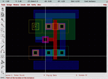
2. Move the instance to the desired location.
Once you have selected the instance, the cursor will show a ghost image representing the instance, and you'll be able to move the instance to the desired location:
3. Place the instance.
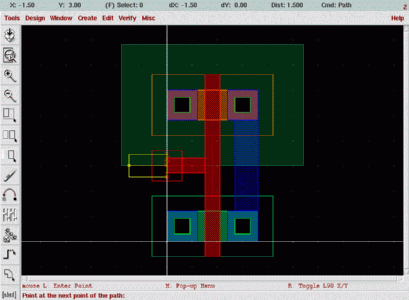
Once satisfied, you can click to place the instance. You'll remain in the instance mode after you have placed the instance, press "ESC" to go back to selection mode again. Note that in this example, the n-well contact has been placed right on top of the n-well boundary, which will obviously generate a rule violation. the n-well is simply not wide enough to accommodate both the PMOS transistor and large contact. This will have to be dealt with in the Next step.
4. Make the power connection.
The instance will not automatically connect itself to the power supply rail. This connection has to be made by either a Metal-1 rectangle or path.
In the previous step we tried to place the
n-type substrate contact in the n-well. Since we had drawn the n-well to cover
the P-diffusion at minimum length, the well is not wide enough to accomodate the
additional contact. We must enlarge the n-well, so that it also covers the
substrate contact.
One way to do this would be to simply draw an adjoining rectangle using the n-well layer. Instead, we will try to modify the existing rectangle, so that it covers the contact.
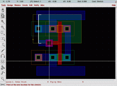
1. Select edit -> Stretch and highlight the left side of the nwell.
2. Move cursor over the left edge of the n-well.
You'll notice that as soon as the cursor is close to the edge, only the edge line will be highlighted as a pale dashed line.
3. Click once to select the edge.
3. Move mouse over the selected edge (without pressing any mouse buttons).
You'll notice that the cursor changes shape when you are close to the edge.
4. Press and hold left mouse button when cursor changes above the selected edge.
You have grabbed the edge, and as long as you do not release the mouse button you can "stretch" the edge. Move the edge of the n-well so that all the of the substrate contact is covered by n-well.