Back to Manual Layout Tutorial
The layout must be drawn according to strict design rules. After you have finished your design, an automatic program will check each and every feature in your design against these design rules and report violations. This process is called Design Rule Checking.
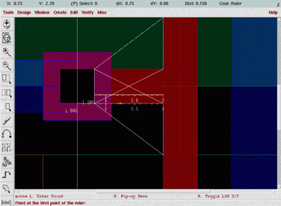
Our design is finished, we must now perform a Design rule Check to see if we have any errors.
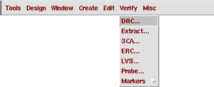
1. From the menu Verify select option DRC
( Check --> DRC )
This will pop-up the DRC options dialog box.
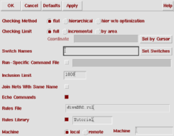
2. Start DRC
The default options for the DRC are adequate for most situations. DRC results and progress will be displayed in the CIW.
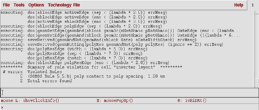
You'll have to check the results from the CIW. In this example we have two poly-to-poly contact spacing errors.
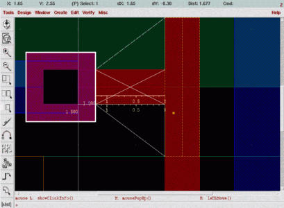
The errors are also highlighted on the layout.
As it is mostly the case, one misplacement will cause multiple DRC errors. The error can be corrected by moving the contact further to the left.
After moving the contact to the left, we will have to perform another DRC.
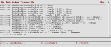
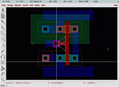
This is a successful DRC.
This is the completed layout of the CMOS inverter.
Congratulations!!
