![]()
Note: The figures given may slightly change from what you see. They will be almost similar if not you will be helped
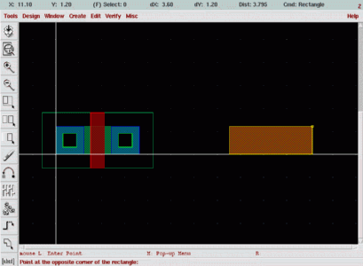
Now that we have drawn the NMOS transistor, the next step is to draw the PMOS transistor. The basic steps involved in drawing the PMOS are the same.
1. Select pactive layer from the LSW
![]()
2. Draw a rectangle 1.44u by 0.36u
You can use the cursor keys and the zoom function to find yourself a place to build the transistor. Make sure you leave enough separation between the NMOS and the PMOS. Note that the PMOS transistor will also be surrounded by the N-well region.
These three steps are identical to the ones done for the NMOS.
1. Draw the gate poly that is 0.96um vertical and 0.24um horizontal.(0.60um from either sides of the active diffusion.)
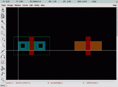
2. Place the contacts(Same dimensions that have been used for drawing the nmos)
3. Cover contacts with Metal-1

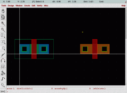
As with the NMOS transistor, the p-type doping (implantation) window over the active area must be defined using the p-select layer.
1. Select pselect layer from the LSW
![]()
2. Draw a rectangle that extends over the active area by 0.24u (2 lambda) in all directions.
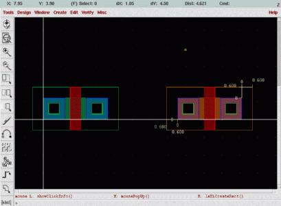
In this process, the silicon substrate is originally doped with p-type impurities. NMOS transistors can be realized on this p-type substrate simply by creating n-type diffusion areas. For the PMOS transistors however a different approach must be taken: A larger n-type region (n-well) must be created, which acts like a substrate for the PMOS transistors.
From the process point of view, the n-well is one of the first structures to be formed on the surface during fabrication. Here we chose to draw the n-well after almost everything else is finished. Note that the drawing sequence of different layers in a mask layout is completely arbitrary, it does not have to follow the actual fabrication sequence.
1. Select the nwell layer from the LSW
![]()
2. Draw a large n-well rectangle extending over the P-Diffusion

The n-well must extend over the PMOS active area by a large margin, at least 0.72u (6 lambda)