![]()
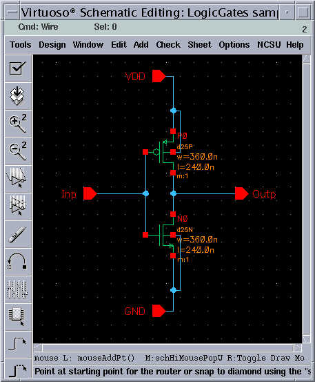
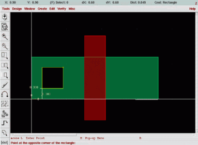
Now we will start drawing our first transistor. which will be the NMOS transistor of the CMOS inverter. From the schematic, we know that this transistor has a channel width of 0.36u. The width of the transistor will correspond to the width of the active area. We will select the n-diffusion layer and draw a rectangular active area to define the transistor.
1. Select nactive layer from the LSW
![]()
2. From the Create menu in Virtuoso select Rectangle
( Create --> Rectangle )
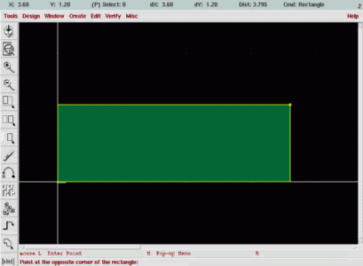
3. Draw the box
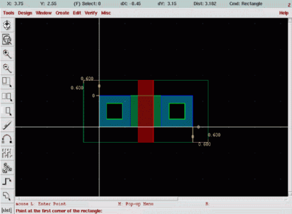
You are now in rectangle mode. Select the first corner of rectangle in the layout window (you may select any point within the window but try to select a point close to the origin), click once, and then move the mouse cursor to the opposite corner. Using the information bar, draw a box that is 1.44u horizontal and 0.48u vertical. All units are in micrometers by default. To simplify the drawing, a grid of half a lambda is used, that is the cursor moves in 0.06u increments only. (The figure may not be to scale)
The second step is to draw the gate. We will use a vertical polysilicon
rectangle to create the channel. Note that the length of the transistor channel
will be determined by the width of this poly rectangle.
1. Select poly layer from the LSW
![]()
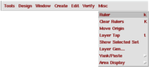
2. From the menu Misc choose Ruler
( Misc --> Ruler )
The ruler is a very handy function. In our case we need to draw the poly rectangle in the middle of the diffusion region. Furthermore, design rules tell us that poly must extend at least by 0.30u (2.5 Lambda) from edge of the diffusion . To pinpoint the location of the poly gate we can use two rulers. One ruler will be used to determine the horizontal distance of the poly gate from the diffusion edge, while a second ruler will show the minimum amount of poly extension outside the diffusion according to the design rules. The poly must be 0.60um from either edge of the active diffusion in the horizontal direction.
3. Draw poly rectangle

The starting point is pinpointed by two rulers. The rectangle function is used to draw a poly rectangle that is 0.24u horizontal and 0.96u(0.30um above active diffusion on both sides) vertical.
The next step is to make the active contacts. These contacts will provide access to the drain and source regions of the NMOS transistor.
1. Select the cc (Active Contact) layer from the LSW.
2. Use the ruler to pinpoint a location 0.12um from the edges of diffusion i.e. the left side or the diffusion to the left of poly.
3. Create a square with a width and height of 0.24um within the active area.
4. From the Edit menu choose Copy
( Edit --> Copy )
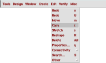
You could choose to draw the second contact the same way as you have drawn the first one. However, copying existing features is also a viable alternative.
5. Copy the contact
After you enter the copy mode, an object must be selected. Click in the contact, you'll notice that the outline of contact will attach to your cursor. Now move the object, and click when you are satisfied with the location.
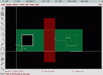
Design rules state that the minimum contact to poly spacing must be 0.24u (2 lambda). You can use a ruler to pinpoint the location. Please note that you can interrupt any mode for placing a ruler (and zooming in and out). After you are finished (by hitting "ESC" key) you'll return to the mode you were in.
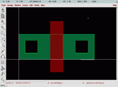
Now you have placed an active contact each into the source and drain diffusion regions of the transistor.
Active contacts in fact only define holes in the oxide (connection terminals). The actual connection to the corresponding diffusion region is made by the Metal layer.
1. Select layer Metal-1 from the LSW
![]()
2. Draw two rectangles (0.48u X 0.48u) wide to cover the contacts
Note that Metal-1 has to extend over the contact in all directions by at least 0.12u (1 lambda). Cover the metal1 region by active diffusion layer so that the contact is covered by active all the sides. Draw a rectangle that is 0.48um horizontal and 0.12um vertical of active.
Each diffusion area of each transistor must be selected as being of n-type or p-type. This is accomplished by a defining the "window: of n-type (or p-type) doping (implantation), through a special mask layer called n-select (p-select).
1. Select nselect layer from the LSW.
![]()
2. Draw a rectangle extending over the active area by 0.24u (2 lambda) in all directions.
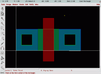
This is it ! Our first transistor is finished, now let us make a few million more of the same :-)