Simulation Using Spectre and Spectre/Verilog
Step 1 : Open a new schematic design
Note : You should first create the symbol of the circuit
schematic which you want to simulate.
If you did not have the symbol for the schematic, refer to the "Create
Symbol" in the “Schematic” tutorial.
1. Open a new schematic.
Follow the same procedure described in "Open a New Schematic" to create a new schematic where you will put your simulation schematic for the inverter. Give a name to your new schematic which makes it clear that the new schematic is to simulate the inverter. The new schematic is called "invTest" in this example.
Step 2 : Select and place components
Note : At this point, you should have an empty schematic editor window open.
1. The first step is to add and to place the components which will be used to simulate the inverter.
The components we need for the simulation of the inverter are the following
:
|
* |
inverter |
Symbol created for the inverter |
|
* |
GND |
Ground line |
|
* |
vdc |
DC voltage source |
|
* |
vpulse |
Pulse waveform generator |
|
* |
C |
Capacitor |
Adding and placing components in a schematic was explained previously . Here you will see how to pick up a symbol you created from your library, and to place it in your schematic.
2. Click Add and select Component.
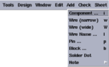
A pop up window will appear
Click Browse in the Add Component window to activate the Component Browser.
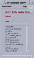
3. You should pay attention to the library from which you take the components.
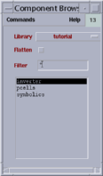
The point where you have to take care of is picking up the components from the correct library. You can change the component library simply by clicking and holding the left mouse button on the library field. In this step, we have two source libraries, one is the given component library "NCSU_Analog_Parts", and the other is our design library which contains the components that we designed stored previously. This library's name in our example is "LogicGates". This means, to pick up the inverter symbol, we have to change the library of the Component Browser to our library, "LogicGates". This can be done, as explained in previous steps by clicking and holding the left mouse button until you select the corresponding library in the pop-up library list.
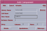
After the library "LogicGates" is selected, there will be a new list of components which are included in this library. Every symbol that you created within this library will show up here. So, by clicking on "inverter" in the component list in the Component Browser, you can pick up the symbol you created for the inverter.
You can always check the corresponding fields in the Add Component window to make sure that you selected the desired component. This can be easily seen in the image below.
You can go to the schematic window and place the symbol of the inverter to a point by clicking on it. These image below show the symbol after placement.
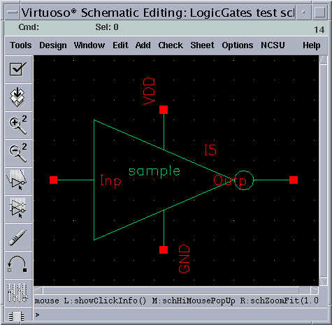
We are now finished placing the symbol of the inverter. Placement of the other components will be explained in the next step.
Step 3 : Select and place components
Note : You do not have to place the components exactly the same way as seen in the example images. As long as you connect them correctly, you can always move a component to some other location in the same schematic.
1. Pick up and place the rest of the components required for the simulation.
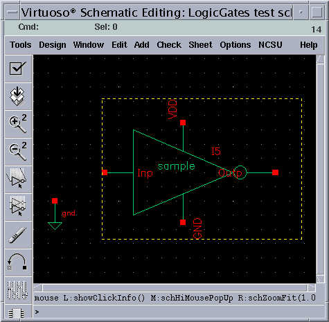
The remaining components are in the "NCSU_Analog_Parts" library. Change your library from "LogicGates" to "NCSU_Analog_Parts".
Open the folder "Supply_Nets", select "gnd" and place them anywhere in the schematic window. The figure after placement is shown below
Go up one folder to the main content folder i.e the "NCSU_Analog_Parts" library window. Open the folder "Voltage Sources", select "vdc" and "vpulse" and place them in the schematic window.
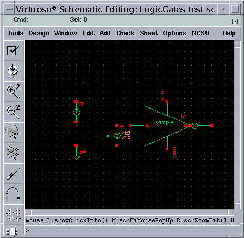
Go up one folder to the main content folder. Open the folder "R_L_C", select "cap" and place it in the schematic window.
We placed all the necessary components for this schematic.
2. Why did we put these components into this schematic ?
You can think of this procedure (creating a new schematic and placing these components into the new schematic) as being analogous to building a "test-bench" for the circuit you designed. As in the real test-bench case, you must build a simple test set-up (consisting of voltage sources, load devices, etc.) around your original circuit to measure its operation and its characteristics.
Step 4 : Wire components
Note : Always save your designs if you make any changes on it. If you make a mistake, you can use the undo command under the edit menu.
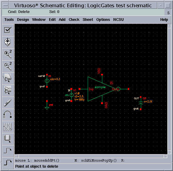
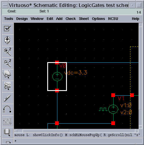
1. Connect the DC-voltage source "vdc + " terminal to "VDD" pin and "vdc -" terminal to "gnd".
A DC-voltage source called "vdd" is required as the power supply voltage in all digital circuits. The value of this voltage usually depends on the technology used. The technology we use for this example is TSMC 0.24uM Deep, which is low-voltage process meaning that the typical VDD voltage value is 2.5 V.
To supply the VDD voltage to the circuit, we will use a DC-voltage source with a constant voltage value of 2.5 V. How to configure the voltage value of the source will be explained in the next steps. The connections of the voltage source are shown in the image below. Simply wire the "VDD" pin with the positive terminal of the DC-voltage source and the "gnd" with the negative terminal of the voltage source.
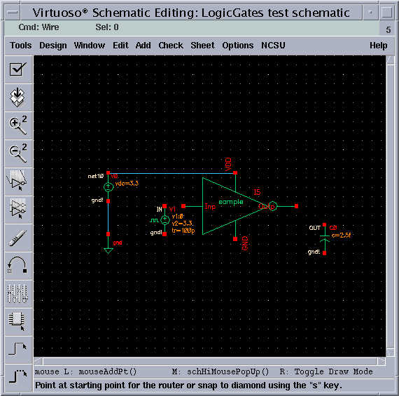
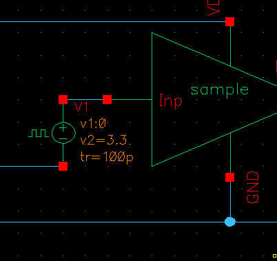
2. Connect the pulse waveform generator "vpulse" to the input of the inverter "Inp".
The pulse generator is a voltage source which can produce pulses of any duration, period and voltage levels. This source will be used to generate the input data (stimuli), so that we can observe the output of the inverter and see if the inverter operates correctly.
Wire the positive terminal of the pulse generator to the input pin of the inverter "Inp" and then the negative terminal of the pulse generator to "gnd".
For the sake of simplicity, you can also pick up more "gnd" components and put them into your schematic where it is needed. All nodes connected to the "gnd" symbol will be short circuited throughout the schematic, i.e., all of them will stay at the reference voltage level which is 0 V (zero volts) or we can connect to the same "gnd" terminal.
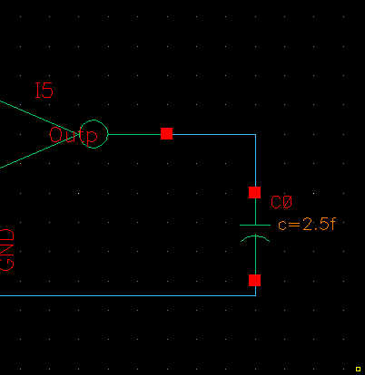
3. Connect the load capacitance "cap" to the output of the inverter "Outp".
In CMOS digital circuits, the output nodes are typically loaded by purely capacitive loads. One of the important specifications of a circuit would usually be its driving capability for a given capacitive load. The larger the capacitive load at the output, the larger the delays to drive this load.
Wire the positive node of the capacitance to the output pin of the inverter "Outp" and then the negative node of the capacitance to "gnd".
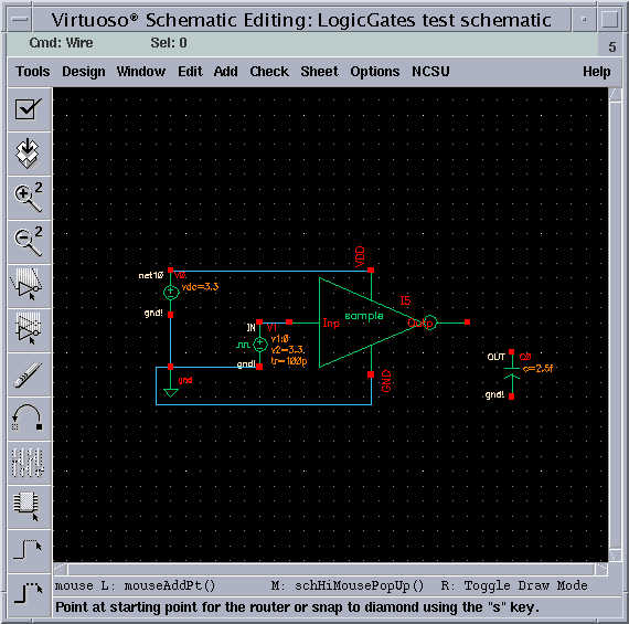
The connections in the schematic below describe the same circuit as in the schematic shown above.
4. At the end of these steps, your entire schematic looks like the following.
Step 5 : Define the voltage sources
In this step, we will enter the necessary parameters for the voltage source components.
1. Edit the properties of the DC-voltage source.
Select the DC-voltage source by clicking on it. The selected component is highlighted by a bright box (rectangle) around it.
Click Edit on the menu bar and select Properties and Object, respectively.
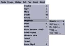
The Edit Object Properties window appears.
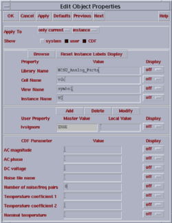
Edit the DC voltage field in the Edit Object Properties window and type the value which is 2.5 v in our examples in the DC voltage row.
Click the "OK" button on the Edit Object Properties window. You can observe the new value entered for the DC-voltage near the DC-voltage source.
2. Edit the properties of the pulse generator
Select the pulse generator instance in the schematic.
The Edit Object Properties window for the pulse generator appears.
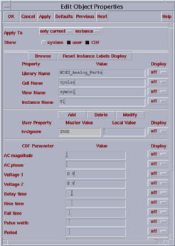
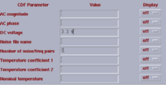
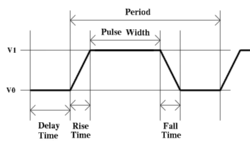
The parameters which are listed in the image above are used to define a pulse which will be repeated periodically. How to use these parameters to define the input pulse waveform is explained in the figure below.
The following image shows the values for the pulse generator parameters which are used to define the input waveform. Click on OK to apply these changes and close the Edit Object Properties window. The voltage 1 is 0 v , voltage 2 is 2.5 v, Delay time is 3n s, Rise time is 100p s and Fall time is 100p s.
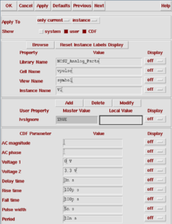
Finally, the new values for the important parameters of the pulse generator appear near the its instance.
Step 6 : Determine the output load
1. Edit the properties of the capacitor which is the output load of the inverter.
Select the capacitor by clicking on it.
Click edit on the menu and select Properties and Object, respectively. The Edit Object Properties window appears. This time, the listed parameters are valid for the selected capacitor.
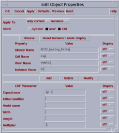
The only parameter we change is the capacitance. As shown in the previous image above, the default value for the capacitance is 1p F (picofarads). This value may be too high for a typical inverter load in this technology. Refer to the "Commonly Used Prefixes for Units in Cadence". By editing the corresponding field in the Edit Object Properties window, we change the capacitor value to 2.5f F (femtofarads).
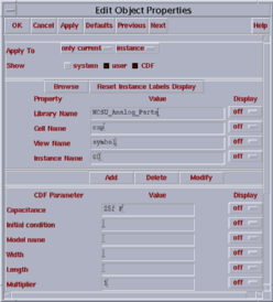
Click on OK in the Edit Object Properties window. The capacitance will be updated to the new value which is 2.5f F.
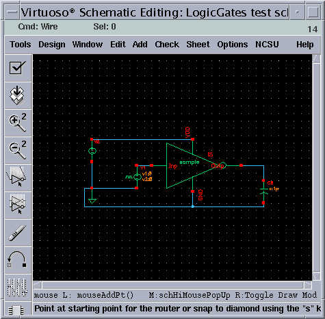
2. Add labels to the nodes you want to observe after the simulation.
In Cadence, labeling a node corresponds to adding certain names to the wires. In our example, there are two important nodes (or wires) which we want to observe during our simulations. These are the input and the output nodes of the inverter. You may think that you labeled these nets before while you were drawing the schematic for the inverter by adding the pins. But, those labels are only valid in that schematic which is now in the lower level of hierarchy. So, every time you create a symbol and use this symbol in a new schematic, you have give new labels to the nodes you want to specify.
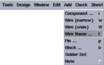
Select Wire Name in the Add command list, as shown below.
The Add Wire Name window appears. Now, you can type all the label names one after the other in the Names field. You will see that there isn't any information related to the direction of the nodes, because only the pins are defined with a direction.
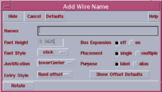
In the example, we will label the two wires as "in" and "out".
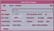
After all the labels are typed, move the mouse cursor on the schematic. Now you will see the first label floating with the mouse cursor. Click on the corresponding net to name the net with this label. As soon as you put the first label, the second label will appear on the mouse cursor. This procedure is repeated until you are finished putting all label names you entered in the Add Label window.
Close the Add Label window either by clicking on OK in the window or pressing ESC on keyboard.
Save your design by using Check and Save in the Design command list. Be sure that the CIW doesn't report any errors or any warnings
Step 7 : Open the simulator window
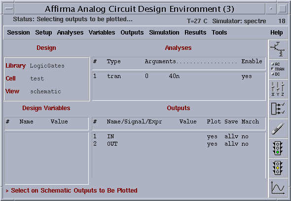
Now, we are ready to simulate our design. We will use Analog Artist as the simulator.
1. Open the Analog Environment window.
Click on Tools in the menu banner of the schematic entry window and choose Analog Environment.
The Analog Environment main window will appears, as shown below. The main fields in this window which we are going to use are.
- Setup
- Analyses
- Outputs
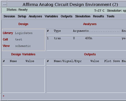
Note that the library, the cell and the view names are listed in the Design field, so that you can check that you are simulating the desired cell using the correct view.
Step 8 : Edit the Simulation Parameters
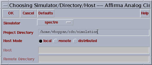
1. Click on Setup in the menu banner and select Model Libraries.
Type in "$MODS/typ" and click on "add". You will observe that the library will be added. To save it click on "OK".
Also in the same Setup, click on Simulator/Directory/Host and select the simulator to be "spectre"
2. Click on Analyses in the menu banner and select Choose.
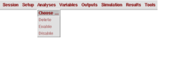
The Choosing Analyses window appears where you can choose the simulation type.
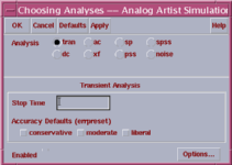
2. Click on tran in the Analysis field.
There are many available analysis options you can choose. Each of these options provides a specific sub-region within the Choosing Analysis window. Since we want to obtain the delay information for the inverter, we choose the transient simulation type, so that the output can be traced in time domain. This may be a little bit different from what you see but it will differ much)
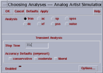
In the Transient Analysis region, type a value in the Stop Time field to determine how long the simulation will take place. The Stop Time is chosen 40n s (nanoseconds).
Note : Do not leave any space between the numeric value and the unit.
Do not type "s" after the unit where "s" stands for
"seconds".
Do not forget to type a unit after the numeric value, otherwise, the
stop time for the simulation will be something in seconds which means your
simulation will last forever !
3. Click on OK in the Choosing Analyses window to close it and to go back to the Analog Environment window.
Step 9 : Run the Simulation
Now, we have to select the nodes that we want to observe as simulation results.
1. Click on Outputs in the menu banner, select To Be Plotted and then Select on Schematic.
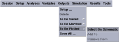
The schematic window becomes active, so that you can select the nodes to be observed in that window
The selected nodes are the input of the inverter, "in", and the output of the inverter "out" which drives the capacitive load. Each time you select a node, the corresponding wire name appears in the Outputs list.
3. Press ESC to finish your selections.
4. Start the simulation by clicking Simulation and then selecting Netlist & Run.
The waveform window appears after the simulation is completed. It includes the waveforms of the selected nodes plotted between t=0 and the determined Stop Time which is 40 ns in our example.
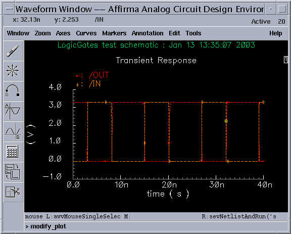
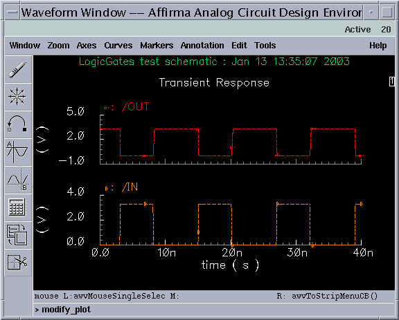
You will see the two waveforms together, plotted on the same time axis. To separate the waveforms, from the menu Axes select option To Strip. Once seperated you can select the waveforms by clicking on them and draging them on top of each other to group. To return to the initial composite waveforms, from the menu Axes select option To Composite. Notice that this option has replaced the former To Strip option.
Step 10 : Re-run the Simulation
If you are not satisfied with the simulation results, there are two different aspects that can be modified :
- The simulation environment is not satisfactory.
This means that the setup to simulate your design should be modified. You can basically change two things, the properties of the input signal you feed to the circuit and the amount of output load which is capacitive. Also, make sure that the power supply voltages are connected properly.
Refer to the step "Define the voltage sources" to setup your input sources.
Refer to the step "Determine the output load" to change the capacitance value of the capacitor.
Refer to the step "Define the voltage sources" to check the connections of your power supply voltages.
These changes are made without descending to a lower level of hierarchy in the design.
- You have to modify your circuit design.
Usually, you will need to change the W/L ratios (the ratio between the channel width and channel length) of the transistors to meet your design specifications. Therefore, you have to edit your design which consists only of a CMOS inverter in our example.
The procedure describing how to re-run the simulation after editing the design is summarized below
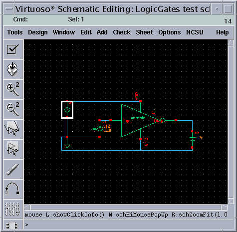
1. Go back to the schematic window and select the symbol of your design. The symbol for the inverter should be selected in this example.
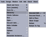
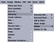
2. Click on Design in the menu banner, select Hierarchy and then Descend Edit.
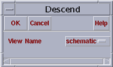
3. Click on OK in the Descend window which asks the designer which view of the design is to be edited.
The existing schematic window now displays the schematic view for the inverter, by going one level down through the design hierarchy.
4. Make the appropriate changes in the editable schematic of the design.
To change the existing W/L ratio for a specific transistor, you have to edit its object properties. Refer to the "Edit Object Properties" step in the schematic example.
5. Check and save your new schematic.
6. Click on Design in the menu banner, select Hierarchy and then Return.
Never forget that you are editing the design at a lower level of the hierarchy - you always must return to the original level from which you have descended.
7. Go to the Analog Environment window and run the simulation again, as described in "Run the Simulation" step.
As the simulation runs, you can switch to the waveform window, because the waveforms will be updated after the simulation is finished.
You can iterate on your design as described in this section of the tutorial. When you want to end the simulation, quit the Analog Artist simulator. This will automatically close the Waveform window, too.
Note: Quitting a tool does not mean closing the corresponding window. Please always use the "close" or "quit" commands located in the menu bar of the tool.
Home Work: Simulate the 2-Input Nand Gate and you have to show all the possible combinations of input and output in the wave form window
Note: The tutorials are taken from Worchester Polytechnic Institute and are modified ECE484 class Spring 2004