Example : Schematic Capture (CMOS Inverter)
Step 1 : Open a new schematic window
Note : Before you begin with going through this example, be sure that you have the Library Manager open.
To open the library manager Do this
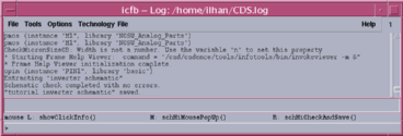
a) Type icd at the console window .This is what you need to
type in everytime to get the
ic configuration window.As soon as you
type icd at the console you should get
something
like this.
Loading NCSU version of TSMC process.
b) Now Go to Tools in icd/icfb window and and select
the Library Manager.
These are the steps that are to be followed to create a library and have to be
done only ONCE.
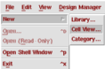
Go to File in Library Manager and select
New Library and Create a Library
“LogicGates” and attach TSMC
0.24u library to it.
Now LogicGates will appear in the library list.
1.Click File on the menu banner in the Library Manager and hold the left mouse button until you choose New and then Cell view.
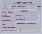
A small new window called "Create New File" appears.
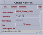
2. There are four main fields in the Create New File window:
- Library Name
You have to choose your working directory by clicking and holding the left mouse button on the Library field. Since our library name is "LogicGates" in this example, we choose the corresponding label, "LogicGates".
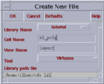
- Cell Name
Enter the name of your cell for which you will draw the schematic. In our example, we will draw the schematic of an inverter, so we type "inverter" in the Cell Name field.

- View Name
The View Name indicates the level of the design hierarchy. You can determine that you are going to draw either a symbol or a schematic or a layout in this field just by typing the corresponding view name. Since we will draw the schematic of an inverter, the correct view name choice is "schematic" for our example.
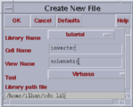
- Tool
Here, you have to select the design editing tool that you will use to enter your design. The tool depends on the hierarchy level of your design. If you click and hold the left mouse button on the tool field, you will see the available tools. Only three of these tools will be used for all the examples.
|
Composer Schematic |
: Schematic editor |
|
Composer Symbol |
: Symbol editor |
|
Virtuoso Layout |
: Layout editor |
Since we will draw a schematic, we choose "Composer Schematic". Choosing Composer Schematic automatically converts the View Name to schematic. Actually, the selected tool converts the View Name to the corresponding one.
3. Now, click on "OK" to close this window and it will automatically open the new schematic editor window chosen in the "Create New File" window.
Step 2: Add components
Note: At this point, you should have an empty schematic editor
window open.
1. The first thing to do is to add and place components which will be used in the schematic.
The components we need for a schematic of an inverter are the following:
- PMOS : p-type MOSFET
- NMOS : n-type MOSFET
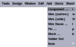
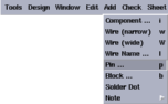
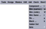
To add components, click on Add in the menu banner of the
schematic entry window and choose Component, as shown below.
(Add -->Component) or the short key "i".
2. A new pop-up windows appear.
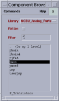
The window is the "Component Browser", which enables the designer to browse easily through the available libraries and select the desired components.
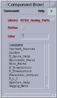
Component Browser pops up every time the Browse button on the Add Component window is clicked.
3. We begin picking up the components by selecting the MOS transistors from the Component Browser window.
You must be careful to pick up the components from the correct library. You can change the component library simply by clicking and holding the left mouse button on the library field.
The correct library is "NCSU_Analog_Parts", so, select this library if it is not selected when you opened the Component Browser. After all, the window should appear like shown above.
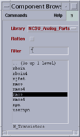
There are many folders under this library. Each of them is named depending on the components they include. So, to pick up an n-type MOSFET, you have to open the "N_Transistors" folder by clicking once on it. The new folder contains many symbols which are also shown in the picture below. Pick up the NMOS transistor by clicking once on "nmos4", which is a model for a four terminal n-type MOSFET.
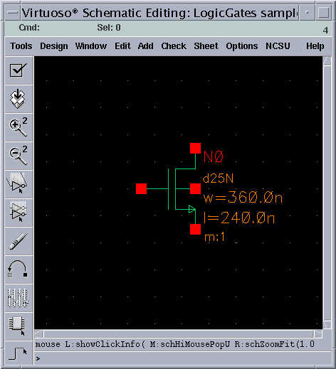
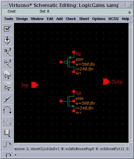
If you move the mouse cursor on the schematic window, you will see a bright NMOS transistor symbol moving with the mouse pointer showing the gate terminal of the transistor. At this point, you decide where to put this transistor. Click on a location in the schematic window, where you want to put the transistor. Please refer to the images below to see a “placed transistor".
The same procedure can be applied to select and to place the PMOS transistor. The only difference is to pick "pmos4" from the "P-Transistors" folder in the Component Browser. The "select-and-place" procedure for PMOS is summarized below.
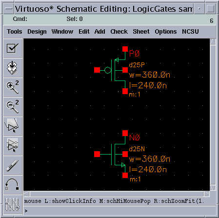
Note: Always make sure that you are not confusing a PMOS transistor with an NMOS transistor. The differences between the PMOS symbol and the NMOS symbol are:
· There is a tiny circle at the gate terminal of PMOS transistors.
- The direction of the arrow which always marks the source terminal of the transistor is different. The arrow points from the source terminal towards the transistor in the PMOS symbol, while it points out towards the source terminal in the NMOS symbol.
Step 3: Placing the pins
You must place I/O pins in your schematic to identify the inputs and the outputs. A pin can be an input or an output or an input-output (bi-directional) or a switch pin. We will only use an input pin and an output pin in our inverter schematic.
1. Click Add on the menu and then select Pin on the pull-down menu or press the short key “p”.
2. The Add Pins window appears.
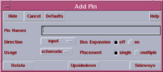
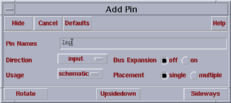
3. Enter the name of your input pin in the Pin Names field.
The input name in this example is "Inp" (note that the pin names can be completely arbitrary). Also, note that the Direction option is set to Input indicating that the current pin is an input pin. As long as you enter pins of the same direction, you can enter pin names one after the other in the Pin Names field, only putting space between them. In this case, each time you place a pin, the next one will appear until all your pins are placed in the schematic.
4. Move the mouse cursor on the schematic window to place pin.
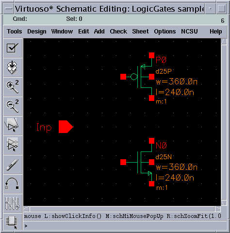
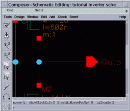
Now, you have your input pin with the name "Inp" floating in the schematic window. Point to a location to place the input pin. Since the input is the gate terminals of both transistors, it is more convenient to put this pin in front of the common node of these terminals.
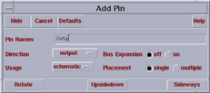
4. Go back to the Add Pin window to pick up an output pin.
First, you have to change the pin direction to Output. To do this, click the left mouse button on the Direction field and select Output in the pop-up menu. Enter the output pin name, which is "Outp" in our example.
5. Place the output pin by clicking on a location in the schematic window.
The procedure is completely analogous to the placement of input pins. Now it is better to put the output pin near the common drain node which is the output of the inverter circuit.
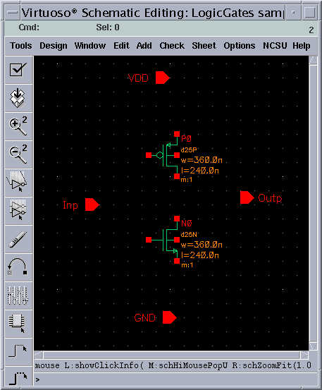
6. Place the VDD and GND pins
It is a better practice to place the
pins for “VDD” and “GND” and force them instead using the instances from the
“add component”.
Go back to the Add Pin window
to pick up a supply pin.
First, you have to change the pin direction to “input”. To do this, click the left mouse button on the Direction field and select “input” in the pop-up menu. Enter the supply pin name, which is "VDD" in our example.
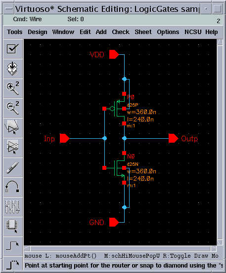
Follow the same procedure for placing the “GND” pin also. The figure after placing all the pins is shown below.
Step 4: Wire components (making connections)
1. After all the components are placed, they should be connected according to the function they realize.
To connect the components in a schematic, we use wires by choosing Add
and then Wire (narrow) on the menu banner.
(Add --> Wire (narrow) )
This command initiates the wiring mode.
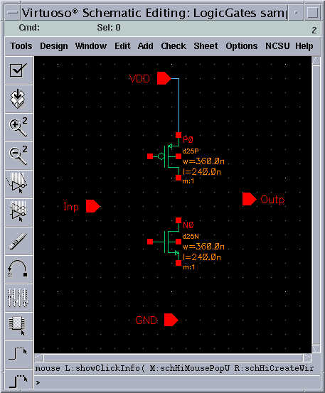
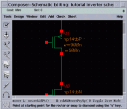
2. We begin to wire the components by connecting VDD and the source terminal of the PMOS transistor.
Every component has tiny red squares on its terminals where you can do the wiring. Connecting any two nets in the schematic is done by first clicking at one of the nets and then at the other one.
During these steps, you will always be prompted by the schematic window. The message appears in the bottom most field of the schematic window. If you follow the instructions prompted in that field, you can easily complete your job. In this step, the following phrase will be prompted:
Point at the starting point for the router
Since we begin with wiring the VDD and the source of PMOS, we click first at the center of the red square which corresponds to the source of PMOS net.
One end of the wire is now fixed, and you will realize that the other end floats and moves according to the mouse pointer. You will also see that the nearest net to the floating end of the wire is automatically highlighted. The new prompt is the following:
Point at ending point for the router
3. Click on the target net which is the VDD terminal.
This was the final step of connecting the two nodes. The same procedure can be applied for the rest of the nodes; first choose any two nodes which should be connected. Then, wire them together just by clicking first one of them and then the other.
As long as you are in the wiring mode, you will be prompted about the next step you have to do, as described above. Press ESC on the keyboard, to leave the wiring mode. You will be in this mode, as long as you don't press ESC or choose another command from the menu.
4. The remaining steps are summarized below.
- Click on the source terminal of NMOS.
- Click on the drain terminal
of PMOS.
Click on the drain terminal of NMOS.
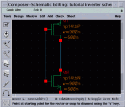
- Click on the bulk terminal of the pmos
and connect to the VDD pin
- Click on the bulk terminal of the nmos and connect to the “GND” pin.
5. Connect the pins to the corresponding nodes using wires.
The wiring procedure is the same as described in the previous steps. Wiring the pins is summarized below:
Click on Add on the menu and then select Wire (narrow). You are now in the wiring mode again.
- Click on the input pin.
=> The other end of the wire is floating.
Click on a point on the common wire which connects the gate terminals of both transistors, PMOS and NMOS.
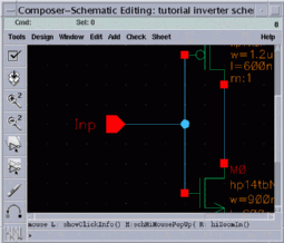
- Click on
the output pin. => The other end of the wire is floating.
Click on a point on the common wire which connects the drain terminals of both transistors, PMOS and NMOS.
- Press ESC to close the wiring mode.
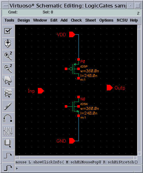
At the end of this step, your schematic should look like the following:
Step 5 : Edit properties of components
The components you select and place from the library always come with a set of default parameters or properties. You can (and usually should) modify component properties according to your design specifications. Here are the steps to edit component properties in the schematic window.
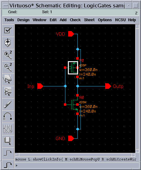
1. Select the PMOS transistor by clicking on it.
The selected component should be highlighted by a bright rectangle (box) around it.
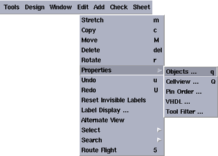
2. Choose Properties and then Object from the Edit menu.
A larger window with many editable fields appears which is called the Edit Object Properties window.
3. Edit the properties by clicking on the corresponding field.
You may change the values for Width or Length depending on your design specifications. Usually, you will change only the Width value, which stands for the channel width, W. The default values for these properties are the smallest available values which are determined by the current technology.
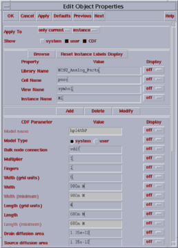
To edit the channel width of the transistor, click on the Width field. Then enter a new value which is either a result of your calculations or just an initial value to see how the performance changes depending on this variable. While changing a parameter, you have pay attention to the unit you use (click here for the list of units). The channel width is changed to 360nm (nanometer) which is equal to 0.36 um (micrometers).
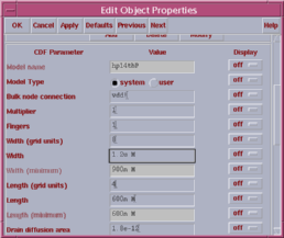
4. Click OK after editing the properties in the Edit Object Properties Window.
The most important parameters (type, dimensions) always appear in the schematic window. You can easily observe the changes of these properties that are listed near the corresponding transistor in the schematic.
Step 6 : Check and Save
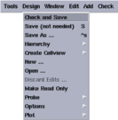
1. Click Design on the menu banner and then select Check and Save.
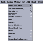
During this tutorial, you may save your design selecting Save on the Design menu. It is also strongly advised that you save your designs frequently, every time after you make significant changes, so that you don't loose your data because of a computer crash or because of a mistake that can happen in a complicated design environment such as this one.
2. Check the message field in the CIW window to see the error and the warning messages.
You can see the message in the screen-shot above indicating that there is no error in our schematic. If this wasn't the case, the errors would have been listed in this window. Check the message field every time you save a design.
Creating a Symbol
Step 1: Opening an existing schematic
Note : You can skip this step if you have your schematic window open.
1. Select your library by clicking on it in the library column of the Library Manager.
The cells in the library will appear in the cell column.
2. Select your cell by clicking on it in the cell column of the Library Manager.
The existing cell views of your cell will appear in the view section. At this point, there should be only the "schematic" view appearing in the "view" column.
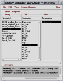
3. Select your cellview by clicking on it in the view column of the Library Manager.
The name of the selected view will appear in the small cell window.
4. In the Library Manager Window, select Open from the File
menu:
( File --> Open )
The schematic of the design will pop-up.
Step 2 : Creating cellview
1. From the Design menu, select Create Cellview and then From
Cellview :
( Design --> Create Cellview --> From Cellview )
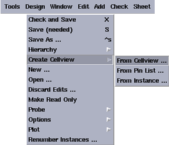
The following window will pop up.
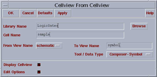
2. Check the view names and click OK
Before clicking OK, you have to ensure that the target view name is symbol, which is indicated with "To View Name" in the bottom-right corner of the pop-up window. If not, then you can change the target view name to "symbol" by clicking and holding the left mouse button on the corresponding box.
Step 3 : Locating the pins
1. After clicking OK in the Cellview From Cellview, window the following window pops up :
In this window (Symbol Generation Options) you can edit your pin attributes and locations. In the default case, you will have your input(s) on the left and your output(s) on the right of the symbol.
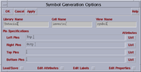
You can change your pin locations simply by putting the pin name in the corresponding pin location field.
2. If you don't want to change anything or you are finished with editing the pin specifications, then press OK to continue.
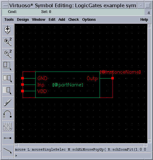
A new window will appear, showing your new symbol. This is the "black box" or symbol representation of your schematic.
Step 4 : Editing the shape of the symbol icon
1. In the new window, the automatically generated symbol is shown.
As seen in the window, the default shape of the symbol icon is a rectangle, with the pins located as defined during the previous step in Symbol Generation Options pop-up window. The small red squares indicate the connection points for each corresponding pin. The red rectangle surrounding the whole symbol determines the clickable area to select the symbol when used in a schematic.
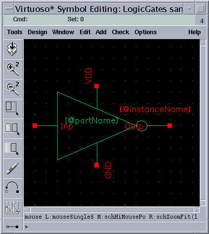
2. If you are not satisfied with the symbol properties, then you can create a new symbol simply by editing the existing one.
You can do the following operations on your symbol :
- Deleting/replacing some existing parts
- Adding new geometric shapes
- Changing the locations for pins and instance name
- Adding new labels
The following is an example for a manually created inverter symbol, which was obtained by editing the symbol above.
Step 5 : Check and Save
1. To check and save the symbol, choose Check and Save from the Design
menu :
( Design --> Check and Save )
While editing the symbol, you can use only Save, which does not check anything. At this point, checking a symbol means comparing the symbol view with the corresponding schematic view, by matching all of the pin names. This occurs only when you click on Check and Save.
Home Work: Repeat the tutorial for an 2-input Nand Gate. You have to enter the schematic in the composer and generate the symbol for the same.
Note: The tutorials are taken from Worchester Polytechnic Institute and are modified for ECE484 class in spring 2004.